Understanding the intricate PCB manufacturing process is crucial for ensuring the reliability and functionality of electronic products. SQPCB, a leading name in the PCB industry, provides a comprehensive guide to the PCB manufacturing process, highlighting each step from design to the finished product.
Understanding PCBs
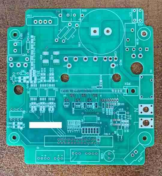
A Printed Circuit Board mechanically supports and electrically connects electronic components using conductive pathways, tracks, or signal traces etched from copper sheets laminated onto a non-conductive substrate. PCBs can be single-sided (one copper layer), double-sided (two copper layers), or multi-layer (multiple copper layers). The complexity of the board often dictates the manufacturing process.
Step-by-Step Guide to PCB Manufacturing
1. Design and Schematic Capture
The PCB manufacturing process begins with a detailed design. Engineers use specialized software (such as Altium Designer, Eagle, or KiCad) to create a schematic capture, which is a blueprint of the circuit. The schematic is then converted into a layout that details the placement of components and routing of electrical connections.
2. Material Selection
Choosing the right materials is crucial for the performance and durability of the PCB. The base material (usually fiberglass-reinforced epoxy resin) and the copper thickness are selected based on the board's application and required electrical characteristics.
3. Creating the PCB Layers
For multi-layer PCBs, the individual layers are created first. This involves:
- Inner Layer Imaging: A photoresist layer is applied to the copper-clad laminate and exposed to UV light through a photomask of the desired pattern. The unexposed areas are then developed away.
- Etching: The exposed copper is etched away using a chemical solution, leaving behind the desired circuit pattern.
- Lamination: Multiple layers are laminated together using heat and pressure to form a single, solid board.
4. Drilling
Precision drilling is performed to create holes for through-hole components and vias (connections between layers). Computer-controlled drilling machines ensure accuracy and consistency.
5. Plating
After drilling, the holes are plated with copper to establish electrical connections between the different layers of the PCB. This step involves:
- Electroless Copper Plating: A thin layer of copper is deposited chemically onto the hole walls.
- Electrolytic Copper Plating: A thicker layer of copper is electroplated to strengthen the connections.
6. Outer Layer Imaging and Etching
The outer layers of the PCB are imaged and etched in a similar manner to the inner layers. A photoresist is applied, exposed to UV light, and developed. The exposed copper is etched away, leaving the circuit pattern.
7. Solder Mask Application
A solder mask, which is a protective layer, is applied to prevent solder bridges between closely spaced solder pads. It also protects the copper traces from oxidation and corrosion. The solder mask is applied, exposed to UV light, and developed to reveal the solder pads.
8. Surface Finishing
Surface finishing ensures reliable soldering and protects the exposed copper. Common finishes include:
- HASL (Hot Air Solder Leveling): A layer of solder is applied and leveled with hot air.
- ENIG (Electroless Nickel Immersion Gold): A thin layer of gold is applied over a nickel barrier, providing excellent surface planarity and oxidation resistance.
9. Silkscreen Printing
Component labels, logos, and other markings are printed onto the PCB using a silkscreen process. This aids in the assembly and identification of the board.
10. Electrical Testing
Each PCB undergoes electrical testing to ensure that there are no short circuits or open circuits. Automated test equipment checks the continuity and functionality of the circuits.
11. Cutting and Profiling
The final PCBs are cut from the production panel and shaped according to the design specifications. This can involve routing or punching out the individual boards.
Quality Assurance and Final Inspection
Throughout the manufacturing process, strict quality control measures are implemented to ensure the highest standards are met. Final inspection includes visual checks, automated optical inspection (AOI), and functional testing.
SQPCB: A Trusted Partner in PCB Manufacturing
SQPCB is renowned for its commitment to quality, innovation, and customer satisfaction. With state-of-the-art facilities and a team of experienced professionals, SQPCB offers comprehensive PCB manufacturing services, from prototyping to large-scale production.
Their dedication to excellence ensures that each PCB meets the stringent requirements of modern electronic applications. For more detailed information on their PCB manufacturing capabilities and services, visit SQPCB.com.
In conclusion, the PCB manufacturing process is a complex and meticulous journey from design to finished product. Understanding each step is crucial for ensuring the reliability and performance of electronic devices. With SQPCB’s expertise and advanced technology, businesses can confidently navigate this process and achieve outstanding results in their electronic products.