A Printed Circuit Board (PCB) is a foundational component in virtually all modern electronic devices, providing the essential infrastructure for electrical connections among various electronic components. PCBs have revolutionized the electronics industry by enabling the miniaturization, reliability, and mass production of electronic circuits. This article delves into what PCBs are, their structure, types, manufacturing process, and their diverse applications.
Structure of a PCB
A typical PCB consists of several layers, each serving a specific function:
1. Substrate
The substrate, often made from fiberglass-reinforced epoxy resin (FR4), provides the mechanical backbone of the PCB. It ensures structural integrity and support for the entire board.
2. Copper Layer
Copper layers are laminated onto the substrate. These layers form the conductive pathways (traces) that connect different components on the PCB. Depending on the complexity of the circuit, a PCB can have one (single-sided), two (double-sided), or multiple (multilayer) copper layers.
3. Solder Mask
The solder mask is a protective layer applied over the copper traces. It prevents short circuits and protects the copper from oxidation. The solder mask gives the PCB its characteristic green color, although other colors are available.
4. Silkscreen
The silkscreen layer is used to print labels, symbols, and component designators on the PCB, aiding in the assembly process by providing visual guidance for component placement.
Types of PCBs
1. Single-Sided PCB
A single-sided PCB has copper traces on one side of the substrate. It is used in simple and low-cost electronic devices.
2. Double-Sided PCB
A double-sided PCB has copper layers on both sides of the substrate, with vias (small holes) connecting the traces on each side. This allows for more complex circuits.
3. Multilayer PCB
Multilayer PCBs consist of multiple layers of copper separated by insulating materials. They are used in complex and high-performance electronic devices like computers and communication equipment.
4. Rigid PCB
Rigid PCBs are made from solid, inflexible materials. They provide structural support and are used in devices where rigidity is required, such as motherboards.
5. Flexible PCB
Flexible PCBs are made from flexible materials that can bend and twist. They are used in applications where the PCB needs to conform to a particular shape, such as wearable devices.
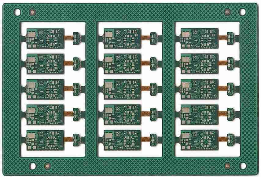
6. Rigid-Flex PCB
Rigid-flex PCBs combine the properties of rigid and flexible PCBs, offering the benefits of both. They are used in complex and compact applications requiring flexibility and durability.
Manufacturing Process
The manufacturing of PCBs involves several key steps:
1. Design
The PCB design process starts with creating a schematic diagram of the circuit. This schematic is then converted into a PCB layout using specialized software.
2. Printing the Design
The PCB design is printed onto a photographic film, which is then used to transfer the design onto the copper-clad substrate through a process called photolithography.
3. Etching
During etching, the exposed copper areas are chemically removed, leaving behind the desired copper traces.
4. Drilling
Holes (vias) are drilled into the PCB to provide pathways for electrical connections between layers and to mount components.
5. Plating and Solder Mask Application
The drilled holes are plated with copper to ensure conductivity. The solder mask is then applied to protect the copper traces.
6. Silkscreen Printing
The silkscreen layer is printed to add labels and component designators.
7. Surface Finish
A surface finish is applied to protect the exposed copper areas and to provide a solderable surface for component placement.
8. Assembly
Components are mounted onto the PCB using either through-hole or surface-mount technology. The assembly process can be automated for high-volume production.
Applications of PCBs
PCBs are ubiquitous in modern technology and are found in a wide array of applications, including:
- Consumer Electronics: Smartphones, tablets, laptops, televisions, and gaming consoles.
- Automotive: Engine control units, navigation systems, and advanced driver-assistance systems (ADAS).
- Medical Devices: Imaging equipment, portable monitors, and implantable devices.
- Industrial Equipment: Motor controllers, power supplies, and automation systems.
- Aerospace and Defense: Communication systems, radar, and navigation systems.
- Telecommunications: Routers, switches, and satellite communication devices.
- Renewable Energy: Solar panels, wind turbines, and energy storage systems.
- Home Appliances: Refrigerators, washing machines, and smart home devices.
- LED Lighting: LED bulbs, strips, and displays.
- Robotics: Robotic arms, drones, and autonomous vehicles.
Conclusion
Printed Circuit Boards are indispensable in the world of modern electronics. Their ability to provide reliable, compact, and efficient connections for electronic components makes them essential across a multitude of industries. From simple consumer gadgets to complex aerospace systems, PCBs form the backbone of countless technological advancements. Understanding their structure, types, and manufacturing process highlights their critical role in today’s technology-driven world.